TEKSTİL LİFLERİ VE KUMAŞTAN TRANSİSTÖR ELDE EDİLMESİ

ACQUIRING TRANSISTOR BY TEXTILE FIBRE AND FABRIC - TEKSTİL LİFLERİ VE KUMAŞTAN TRANSİSTÖR ELDE EDİLMESİ


Proje yazarı :Çağa BİZİMCAN
Patent Nu:2013/ 02276

                                                           SUMMARY
 
         ACQUIRING TRANSISTOR BY TEXTILE FIBRE AND FABRIC
 
The invention is to provide voltage and current acquisition by increasing and decreasing electrical current charged the panels in the mobility emerged along with the replacement made by the pressure and the electrons located outer orbit of atoms composed between the panels P-type and N-type triggering each other through the fabric panels knitted and/or weaved with threads composed of the fibres including reinforced N and P type fibres and/or both N and P types crystals and/or the fibres including reinforced crystals directly and/ or N type and P type  and/or continuous staple by the electricity acquired through natural and artificial ways or all other chemical ways and petroleum and petroleum-derived along with all kind of 
renewable energy
resources especially solar power. 
 
                                                           INSTRUCTION  
 
           ACQUIRING TRANSISTOR BY TEXTILE FIBRE AND FABRIC
 
Technical Area
This invention is to provide voltage and current acquisition by increasing electrical current charged semi conductive NPN type and/or PNP type panels occurred the cell and /or cells constituted by means of reinforced processing of the fabrics in known sewing machine and/or making the technique become knitted fabric and textile fabric in weaving looms and/or knitting machine and/or brode and raschel machines through all kind of conductive metals or conductive fibre or thread or conductive metal thread providing transmission of electrical current and (P-type) and (N-Type) fibres produces within the scope of the invention and/or transistor production providing voltage and current acquisition by increasing electrical current with the threads produced by merging fibre and two and more fibres produced by being doped through saturating and/or doping and/or harmonizing with the elements especially boron with atomic number 5 and phosphorus with atomic number 15 within 3. And 5 group of periodic table by undergoing various chemical process on relatively thin industrial glass called barium aluminoborosilicate and/or derivatives of barium and aluminium element and silicium-boron mixture or Germanium and/or compounds or other all kind of continuous and/or discontinuous fibres with (P-type) and (N-Type) threads produced from silicon and/or glass fibre or fibres up to the highest denier starting from normal or crystallized silicon thread or fibre  and/or normal or crystallized glass fibre or thread or glass wool continuous or discontinuous normal or crystallized 3. group silicon (P-type) and continuous or discontinuous normal or crystallized 5. group silicon (N-Type) nano scale acquired by harmonising or being doped of the compound chemical additive elements and/or 3. Group and 5. Group elements of periodic table related to mono crystallized or crystallized pure silicium or crystallized silicon raw material and/or mono crystallized or crystallized Germanium and/or mono crystallized or crystallized glass raw material within the scope of this invention regarding the electricity acquired through natural and artificial ways or all other chemical ways and petroleum and petroleum-derived along with all kind of renewable energy resources.
In the technical area, in order to increase the conductivity of semi conductive at an ideal and convenient temperature, (P-Type) and (N-Type) semi conductive should be doped with relatively low level – a few ppm - of foreign substance (boron and phosphorus or other elements in the 3rd and 5th group of periodic table) creating gap – holl. As a result of doping this semi conductive, in case semi conductive was being doped by some of silicium or germanium within the crystallized form, atoms of this semi conductive has been replaced by foreign atoms. The process made on these spaces in which the crystallized order of semi conductive is corrupted is called doping. When a semi conductive being doped with a foreign substance creating gap – holl is exposed to voltage as heat, light, power etc externally, and number of free electrons increases highly compared to the situation within the crystal. If the number of free electrons increases through doping, it is called N-type doping; if the number of free electrons decreases and the number of holes increases, then it is called P-type doping.   Either N-type or P-type doping, semi conductive being doped by these foreign substances are called as doping semi conductive.  Through producing Silicium or Germanium or additive substances composed of other semi conductive and N-type and P-type semi conductive fibres and threads composed of them technically, by producing NPN type or PNP type semi conductive panels, acquisition of voltage and current can be provided by increasing electricity current charged to these panels.
 
Former Technique
In case the technique is known, in order to increase all kind and power of electrical current and provide voltage acquisition, apart from (P-Type) and (N-type) Fabric panels produced by fibres and threads within the scope of this invention, other semi conductive being doped by other method and techniques and solid type transistor up to about 100.000 kinds have been produced and used in the industry. 
 
Purpose of Invention
The problem which was tried to solve by this invention is the production of textile based transistor directed towards providing voltage and current acquisition by increasing and decreasing electrical current charged the panels in the mobility emerged along with the replacement made by the pressure and the electrons located outer orbit of atoms composed between the panels P-type and N-type triggering each other through the fabric panels knitted and/or weaved with threads composed of the fibres including reinforced N and P type fibres and/or both N and P types crystals and/or the fibres including reinforced crystals directly and/ or N type and P type and/or continuous staple by the electricity acquired through natural and artificial ways or all other chemical ways and petroleum and petroleum-derived along with all kind of renewable energy resources especially solar power.  
 
Explanation of Figures
The fibres and fabrics and/or all kind of textile knitted by the threads composed through these fibres and/or N-Type and P-Type fibres have been indicated in the figures attached for providing acquisition of voltage and current by increasing electricity current charged to the panels composed of the fibres and additive fibres in order to reach the purpose of this invention.
Figure 1: The model explaining the logic of the process of NPN type transistor produced by conductive metal fibres and N-type and P-Type fibres used within the scope of this invention and transistors made by the substances produced apart from the invention and used. 
Figure 2: Scheme showing the movement direction of the electricity being charged and the fibre composed of semi conductive fibre being doped in NPN type.
Figure 3:  Bending N and P type fibres in the order of NPN.
Figure 4:  NPN type tartan Fabric Panel transistor covered by an isolator substance.
Figure 5:  NPN type Fabric Panel transistor covered by an isolator substance.
Figure 6: The model explaining the logic of the process of PNP type transistor produced by conductive metal fibres and N-type and P-Type fibres used within the scope of this invention and transistors made by the substances produced apart from the invention and used
Figure 7:  Scheme showing the movement direction of the electricity being charged and the fibre composed of semi conductive fibre being doped in PNP type.
Figure 8:  Bending N and P type fibres in the order of PNP
Figure 9 : PNP type tartan Fabric Panel transistor covered by an isolator substance.
Figure 10: PNP type Fabric Panel transistor covered by an isolator substance.
 
Explanation of Figures’ References
1        : N-Type semi conductive fibre. (collector)
2        : P-Type semi conductive fibre.(Base)
3        : N-Type Semi conductive fibre.(Emitter)
4        : The thread composed by bringing N and P type fibres together or bending.
5       : Covering outer surface of fibre or threads with an isolator substance  
6        : N-Type semi conductive fibre (collector)
7        : P-Type semi conductive fibre.(Base)
8        : N-Type semi conductive fibre.  (Emitter)
9        : Warp weft directed sequence of P-Type semi conductive fibres on textile fabric   (Base)
10    : Warp weft directed sequence of N-Type semi conductive fibres on textile fabric   
11    : Warp weft directed sequence of conductive metal fibres on textile fabric or its aspect embroidered 
12    : Warp weft directed sequence of isolator fibres on textile fabric
13    : Electrical current charging key  
14    : P-Type sub fibre group sequence in PNP type transistor (Collector)
15    : N-Type middle fibre group sequence in PNP type transistor (Base) 
16    : P-Type upper fibre group sequence in PNP type transistor  (Emitter)
17    : Covering PNP type transistor group with isolator substance 
18    : P-Type sub fibre group bending in PNP type transistor (Collector)
19    : N-Type middle fibre group bending in PNP type transistor (Base) 
20    : P-Type upper fibre group bending in PNP type transistor  (Emitter)
21    : Covering PNP type twisted transistor group with isolator substance 
22    : Distribution channel through the metal fibre or wire in which the electricity current passing 
23    : The area knitted or weaved by isolator fibre surrounding fabric panel
24    : Warp weft directed sequence of P-Type semi conductive fibres on textile fabric
25    : Warp weft directed sequence of N-Type semi conductive fibres on textile fabric   
26     Weaving or embroidering PNP type transistor fabric panel providing the transmission of electrical current
27    : Covering PNP type twisted transistor group with isolator substance 
      28  : Processing metal fibres or wires through weaving and/or embroidering.
Explanation of Invention:
A- The invention is a textile based transistor device directed towards providing voltage and current acquisition by increasing electrical current charged semi conductive NPN type and/or PNP type panels occurred the cell and /or cells constituted by means of reinforced processing of the fabrics in known sewing machine and/or making the technique become knitted fabric and textile fabric in weaving looms and/or knitting machine and/or brode and raschel machines through all kind of conductive metals or conductive fibre or thread or conductive metal thread providing transmission of electrical current and (P-type) and (N-Type) fibres produces within the scope of the invention and/or transistor production providing voltage and current acquisition by increasing electrical current with the threads produced by merging fibre and two and more fibres produced by being doped through saturating and/or doping and/or harmonizing with the elements especially boron with atomic number 5 and phosphorus with atomic number 15 within 13. and 15 group of periodic table by undergoing various chemical process on relatively thin industrial glass called barium aluminoborosilicate and/or derivatives of barium and aluminium element and silicium-boron mixture or Germanium and/or compounds or other all kind of continuous and/or discontinuous fibres with (P-type) and (N-Type) threads produced from silicon and/or glass fibre or fibres up to the highest denier starting from normal or crystallized silicon thread or fibre and/or normal or crystallized glass fibre or thread or glass wool continuous or discontinuous normal or crystallized 3. group silicon (P-type) and continuous or discontinuous normal or crystallized 5. group silicon (N-Type) nano scale acquired by harmonising or being doped of the compound chemical additive elements and/or 3. Group and 5. Group elements of periodic table related to mono crystallized or crystallized pure silicium or crystallized silicon raw material and/or mono crystallized or crystallized Germanium and/or mono crystallized or crystallized glass raw material.
B-The invention is textile based transistor device covered its outer surface by isolator case directed towards providing voltage and current acquisition by increasing and decreasing electrical current charged the panels in the mobility emerged along with the replacement made by the pressure and the electrons located outer orbit of atoms composed between the panels P-type and N-type triggering each other through the fabric panels knitted and/or weaved with threads composed of the fibres including reinforced N and P type fibres and/or both N and P types crystals and/or the fibres including reinforced crystals directly and/ or N type and P type and/or continuous staple by the electricity acquired through natural and artificial ways or all other chemical ways and petroleum and petroleum-derived along with all kind of renewable energy resources especially solar power.
 
C-  Functioning of NPN type transistor produced by N-Type and P-Type fire or threads is as follows. Formation of NPN type transistor compose of a base substance constituted two N type semi conductive fibres and threads and P type semi conductive fibre and thread located between them as a thin layer. Base layer located between two N type fibre and threads functions for controlling electronic transition. The textile based transistor may enlarge small currents or may ensure a huge receiver functioning with a small current by supervising the current transiting. As it is seen in Figure 1, in NPN type transistors, while anode of Vbb resource charged base pole positively, cathode of Vss resource pushes the electrons in the emitter pole up. The electrons pressed have been pulled by the base. Electrons in the transmittal line of the emitter enter into the base region by exceeding E-B voltage set, however, while about 2-3 % of the electrons coming from emitter region have been pulled by base region due to narrowness of base region, remaining 97-98 % passed to the collector. Anode of Vcc resource pulls the electrons toward collector region and electron flow become continuous and electron flow from emitter to collector continues as long as the base low given by Vbb resource continues.  Electrons go up, holes go down in NPN type transistors and therefore, positive signal implemented to the base passes current from collector towards the emitter. It is known that emitter flow is equal to the sum of base and collector flows.
 
D- Form of PNP type transistor produces with P-type and N-Type fibre or threads is the same as NPN type transistor.  The difference is to locate N type semi conductive fibre and thread between two P type semi conductive fibres and threads as a thin layer. In PNP type transistors, while cathode of Vbb resource charged base pole negatively, anode of Vcc resource pushes the holes charged positively in the emitter pole up. By this way, the ones positively charged and pressed have been pulled by the base and passed towards the collector region. The movement of holes become continuous since cathode of Vcc resource pull the holes in the collector region itself.  This movement towards the collector continues as long as the Vbb flow continues. Electrons go down, holes go up in PNP type transistors and therefore, negative signal implemented to the base transmits current from emitter towards the collector. It is also known that emitter flow is equal to the sum of base and collector flows.
 
Implementation Style of Invention to Industry
The above-mentioned purposes, the electricity produced all kinds of respect for the environment and nature of the invention is safe and additive fibres and the fibres of the panels and install the electric current by increasing the acquisition of voltage and current of the textile based transistor enables this device to ensure easy and safe and it is possible to mount the electronic devices compactly that this product can be obtained and abundant raw materials are those known in nature. The product can be produced in the sector of industry especially in textile and energy and/or any other branch of the industry and can be used in every field and applicable in industry.


                                                           REQUETS 

1)      Invention is(P-Type) fibre production method  and its qualification is; to subject the process of production of continuous or discontinuous (P-Type) fibres in the machines known as the technique for producing textile fibre of semi conductive mono crystallized or crystallized silicium with single or multiple crystals or silicon substance and/or mono crystallized or crystallized glass substance or all other semi conductive elements in periodic table and/or compounds and pure or compound elements from the 3rd group of periodic table (boron, aluminium, gallium, indium, thallium, unutrium, holmium, einsteinium) being doped starting from nano scale to the highest thickness.
 
2)      It is the method characteristics in Request 1; By bringing 2 or more (P-Type) fibres together, to start with the smallest number of similar fibre types and/or nano scaled numbers, to include textile based fibre up to the highest number.
 
3)       Invention is (P-Type) fibre production method and its qualification is; to subject the process of production of continuous or discontinuous type (P-Type) fibres in the machines producing textile fibre known as the technique up to the highest thickness starting from nano scale with one or more doping mono crystallized or crystallized germanium element and pure or compound gallium element from 3rd group of periodic table.
 
4)      It is the method characteristics in Request 3; By bringing 2 or more (P-Type) fibres together, to start with the smallest number of similar fibre types and/or nano scaled numbers, to include textile based fibre up to the highest number.
 
 
5)       Invention is (N-Type) fibre production method  and its qualification is; to subject the process of production of continuous or discontinuous (N-Type) fibres in the machines known as the technique for producing textile fibre of semi conductive mono crystallized or crystallized silicium with single or multiple crystals or silicon substance and/or mono crystallized or crystallized glass substance or all other semi conductive elements in periodic table and/or compounds and pure or compound elements from the 5th group of periodic table (Nitrogen, phosphorus, arsenic, antimony, bismuth, ununpentium) or mono crystallized or crystallized Germanium element with the element Lithium from … group of periodic table being doped starting from nano scale up to the highest thickness.
 
6)      It is the method characteristics in Request 5; By bringing 2 or more (N-Type) fibres together, to start with the smallest number of similar fibre types and/or nano scaled numbers, to include textile based fibre up to the highest number.
 
7)      Invention is (N-Type) fibre production method and its qualification is; to subject the process of production of continuous or discontinuous type (N-Type) fibres in the machines producing textile fibre known as the technique up to the highest thickness starting from nano scale with one or more doping mono crystallized or crystallized germanium element and pure or compound other element from 5th group of periodic table.
8)       It is the method characteristics in Request 7; By bringing 2 or more (N-Type) fibres together, to start with the smallest number of similar fibre types and/or nano scaled numbers, to include textile based fibre up to the highest number.
9) The request is the NPN type textile thread based production method and its characteristics; As it is in the model of Figure 1, by model as in claim 5 and 7, obtained by process step (n-type) two or more twisted fibres among themselves so that the innermost (5) and / or untwisted (1) by treatment assemble and this istem1'deki on fibres obtained by processing steps (P-type) two or more fibres, (n-type) fibres twisted (6) or untwisted (2) wound on any processing and which forms the middle layer (P-type) fibres so that the (n-type) two or more fibres twisted (7) and / or untwisted (3) to be wound on the top as in Figure 2 and Figure 3, by treatment, as in the n-type semi-conductive fibre made ​​of such transactions.
      (collector) (1), (n-type) semiconductor fibre (emitter) (3) arrangement of fibres arranged in a layer between the p-type semiconductor thin fibres (the base) (2) consisting of the series base thereof and the outer surface of the whole insulator assembly coated with the substance (4), (8) consists of NPN type transistor thread. NPN type transistor arrangement of fibres between the two N-type, P-type layer of fibres base (2) to control the passage of electrons through the task of the present invention, the transistor is produced in the form of textile yarn based on his business, or a small current by checking the amplification of small currents is that the operation of a receiver with a large current.
 
10) It is the method characteristics in Request 9; Nano-scale in request 9 to a thickness of the highest starting NPN type transistor-based fibres produced (the base), which forms the P-type fibres (+). (Emitter) constituting the yarn wrapped on top of the N-type fibres (-) poles are connected to the bottom of the wrapped yarn with a given electric charge and the thread (collector) portion of the fibres forming the n-type electron structure by compressing the electricity base in small (+) flows increased by enlarging the (+) supply current, and the thread is no fibre without the burden of poles connected directly to the electrical current sent to the (-) currents amplified by the device (+) flows and loads to be exported as a result of a merger in the end the work is to provide a great receiver. (Figure:1-Figure:2)
     
11) The request is the production method textile thread based PNP type transistor and its characteristics; As in the model of Figure 6, obtained by the processing steps of claim 1 and 3 (P-type) two or more filaments twisted with each other so that the innermost (19) and / or untwisted (15) by treatment of a and commencing upon claim 5, wherein the fibres obtained by the process steps (n-type) two or more fibres (P-type) fibres twisted (20) or untwisted (16) wound on the middle layer formed and any processing of the (n-type) so that the fibres on (P-type) of 2 or more twisted fibres (21) and / or untwisted (17) to be wound on the top as in Figure 6 and in Figure 7 by treatment as with the P-type semiconductor fibre such transactions. (collector) (15), (P-type) semiconductor fibre (emitter) (17) between the assembly of fibres arranged in a thin layer of N-type semi-conductive fibres (the base) (16) consisting of the series base thereof and the outer surface of the apparatus coated with the whole non-conductive material (18), (22) is composed of PNP type transistor thread.
 
12) It is the method characteristics in Request 11; Request 11 to a thickness of the highest starting nano-scale PNP type transistor-based fibres produced (the base) constituting the N-type fibres (-). (Emitter) constituting the yarn wrapped on top of the P-type fibres (+) poles provided with electric charge by connecting the bottom of the yarn and the thread is wrapped (collector) portion of the fibres which constitute the P-type (the base) to the (-) of the load compression electricity with a small (-) flows increased by enlarging the (-) supply current, and the thread is no life without the burden of poles connected directly to the electrical current sent to the (+) currents amplified by the device (-) flows as a result of a large receiver end, the combination of loads and exporting is to work.      (Figure:6 -Figure:7) 
13 ) It is method mentioned in the requests above and its characteristic; 1,2,3,4,5,6,7,8 claim in Figure to form a NPN type transistor 4 and Figures: 5'deki woven fabrics, as in the N-type semiconductor yarns (collector) (1), N-Type Semiconductor yarn (Emitter) (3) arrangement of the warp and weft yarns of the warp and weft yarns formed into a thin layer between the P-type semiconductor (Base) (2) which consists of yarns of yarn strands. N-type semi conductive weft direction on the woven fabric warp arrangement (10) between the P-type semiconductor warp yarns in the weft direction on the woven fabric (the base) layer (9) formed looms or knitting machines, woven and knitted from yarns of yarn knitted insulator edges (12) and conductive metal wires woven yarn or yarns out of insulator and / or may be processed by embroidery (11) N-type semi conductive on the weft yarns in the warp direction of their formation of woven fabric (10), the N-type semiconductor on the fabric, the weaving direction of weft warp array (12) electron and providing passage over the panels are covered with non-conductive material (27) and by the task of checking of the invention, textile weaving or knitting finished his operation based on the current through the transistor by controlling the growth of a small or a small current flows through the operation of the receiver is that it provides a large current.
14) It is method mentioned in the requests above and its characteristic; 1,2,3,4,5,6,7,8 claim in Figure to form a PNP type transistor: and Figure 9: 10, as well as woven fabrics, yarns, the P-type semi conductive (collector) (15) P-Type Semi conductive yarn (Emitter) (17) set up between the warp and weft yarns of the warp and weft yarns are created in a thin layer of n-type semi-conductor (Base) (16) which consists of yarns composed of fibers. P-type semiconductor on the fabric, the weaving direction of weft warp array (26) between the n-type semi-conductive warp yarns in the weft direction on the woven fabric (the base) layer (25) looms or knitting machines to be formed from woven and knitted yarns edges yarn knitted insulator (24) and insulation of the conductor metal thread or wire woven yarns and / or may be processed by embroidery (28) n-type semi-conductive warp yarns in the weft direction of their formation on the woven fabric (25), the P-type semi conductive yarns woven fabric that on the weft warp array (26) providing passage of electrons and the panels are coated with non-conductive material via (27) and acting as a control of the invention, finished woven or knit based textile current through these transistors work done by controlling the growth or small flows the operation of the receiver is that it provides a large current with a small.
 
......................................................................................................................

Patent No:2013/ 02276


                                                           ÖZET


         TEKSTİL LİFLERİ VE KUMAŞTAN TRANSİSTÖR ELDE EDİLMESİ  


Buluş, güneş enerjisi başta olmak üzere her türlü yenilenebilir enerji kaynakları ile petrol ve türevlerinden  ve diğer tüm kimyasal yollarla ya da doğal ve yapay yollarla elde edilen elektriğin , N-Tipi ve P-Tipi  devamlı ve/veya kesikli liflerin ve/veya hem     N-tipi ve hem de P-Tipi katkılı kristalleri içinde barındıran liflerden doğrudan ve/veya N ve P tipi liflerden ve/veya hem N ve hem de P tipi kristalleri içinde barındıran liflerden oluşan iplikler ile dokunan ve/veya örülen kumaş panelleri vasıtasıyla P-Tipi ve N-Tipi paneller arasında oluşan atomların dış yörüngelerindeki elektronların birbirlerini tetiklemesi ve baskısı ile yer değiştirmesi ile oluşan hareketliliğinde bu panellere yüklenen elektrik akımının yükseltilerek veya alçaltılarak akım ve gerilim kazancı sağlanmasıdır.


                                                           TARİFNAME  


           TEKSTİL LİFLERİ VE KUMAŞTAN TRANSİSTÖR ELDE  EDİLMESİ                                        


Teknik Alan

Bu buluş, güneş enerjisi başta olmak üzere her türlü yenilenebilir enerji kaynakları ile petrol ve türevlerinden  ve diğer tüm kimyasal yollarla veya doğal ve yapay  elde edilen elektriğin bu buluş kapsamında ,  monokristalize veya kristalize saf silisyum veya kristalize saf silisyum veya kristalize silikon hammaddesi ve/veya monokristalize veya kristalize Germanyum ve/veya monokristalize veya kristalize cam hammaddesinin periyodik cetvelin 3.grup ve 5.grup elementleri ve/veya bileşik kimyasal katkı elementlerinin harmonizesinden veya katkılanmasından  elde edilen normal veya kristalize silikon lifi veya elyafı ve/veya normal veya kristalize cam lifi veya elyafı veya cam yününden devamlı veya kesikli normal veya kristalize 3.grup silikon (P-Tipi) ve devamlı veya kesikli normal veya kristalize 5.grup silikon (N-Tipi) nano ölçekten başlayıp en yüksek denyeye kadar silikon ve/veya cam lif veya elyaflarından üretilen (P-Tipi)ve (N-Tipi) ipliklerin ile baryum alüminyum borosilikat olarak adlandırılan çok ince bir endüstriyel cam  ve/veya Baryum ve alüminyum elementinin türevlerinden ve silisyum –bor karışımından veya Germanyum ve/veya bileşiklerinden veya diğer her türlü devamlı ve/veya kesikli liflerin çeşitli kimyasal işlemden geçerek Periyodik cetvelin 3.ve 5.grubundan başta 5 Atom no.lu Bor ve 15 atom no.lu fosfor olmak üzere elementlerle harmonizesi ve/veya  katkılanması veya emdirme yoluyla katkılanması ile üretilen lif ve iki ve daha fazla liflerin birleştirilmesi ile üretilen ipliklerle elektrik akımını yükselterek akım ve gerilim kazancı sağlayan transistör üretimi ve/veya buluş kapsamında üretilen (P-Tipi) ve (N-Tipi) ipliklerle ve elektrik akımının iletilmesini sağlayan iletken metal iplik veya her türlü iletken lif veya iplik veya iletken metallerle tekniğin bilinen dokuma tezgahlarında ve/veya örgü makinelerinde ve/veya brode ve rachael (raşel) makinelerinde dokuma kumaş ve örgü kumaş  haline getirilmesi ve/veya bu kumaşların nakış makinelerinde takviyeli işlenmesi  suretiyle oluşturulan hücre ve/veya bu hücrelerden meydana gelen NPN tipi ve/veya PNP tipi yarıiletken panellere yüklenen elektrik akımını yükselterek akım ve gerilim kazancı sağlanmasıdır.

Teknik alanda, uygun ve ideal bir ısıda yarı iletkenin iletkenliğinin yükseltilebilmesi için,     (P-Tipi) ve (N-Tipi)  yarı iletkenlerin  kristal kafesine çok küçük bir miktarda -birkaç ppm kadar-  boşluk-hol-yaratacak yabancı madde(Bor ve Fosfor veya Periyodik cetvelin 3.ncü ve 5 grubundan diğer elementler) ile katkılanması gerekir. Bu yarı iletkenin katkılanması sonucunda kristal yapı içerisinde bazı silisyum veya germanyum yarı iletkeni katkılandı ise bu yarı iletken atomlarının yerlerini yabancı atomlar alır. Yarıiletkenlerin kristal düzeninin bozulduğu bu yerlere yapılan işleme katkılama (doping)işlemi denir.Boşluk-hol-yaratacak yabancı bir madde ile katkılama yapılmış bir yarı iletkene dışarıdan ısı,ışık güç,v.b.gibi gerilim uygulandığında serbest kalacak elektronların sayısı kristalin içinde bulunduğu duruma göre çok artar.Bu katkılanma ile,serbest kalan elektronların sayısı artıyorsa N-tipi katkılanma, eğer serbest elektronların sayısı azalıp, deliklerin (holes) sayısı artıyorsa P-tipi katkılanma denir. İster N-tipi veya P-tipi olsun, bu yabancı maddelerle katkılanan yarıiletkenlere katkılı yarı iletkenler  denir. Bu şekilde katkılanan silisyum veya Germanyum veya diğer yarıiletkenlerden oluşan katkılı maddelerle N- tipi ve P- tipi yarı iletken lifler ve bunlardan oluşan ipliklerin teknik olarak üretilmesi ile NPN tipi veya PNP tipi yarıiletken paneller üreterek bu panellere yüklenen elektrik akımının yükseltilerek akım ve gerilim kazancı sağlanabilir.


Önceki Teknik

Tekniğin bilinen durumunda, her türlü ve güçte elektrik akımının yükseltilmesi ve gerilim kazancı sağlanması için , bu buluş kapsamındaki lif ve ipliklerle üretilen (P-Tipi) ve (N-Tipi) Kumaş panelleri dışında,  başka usul ve tekniklerde  katkılanan yarı iletkenlerle katı ve sert yapıda 100.000’e yakın çeşitte transistör üretilmiş ve sanayide kullanılmıştır.  


Buluşun Amacı

Bu buluşun çözümünü  amaçladığı  problem ,güneş enerjisi başta olmak üzere her türlü yenilenebilir enerji kaynakları ile petrol ve türevlerinden  ve diğer tüm kimyasal yollarla doğal ve yapay yollarla elde edilen elektriğin , N-Tipi ve P-Tipi  devamlı ve/veya kesikli liflerin ve/veya hem N-tipi ve hem de P-Tipi katkılı kristalleri içinde barındıran liflerden doğrudan ve/veya N ve P tipi liflerden ve/veya hem N ve hem de P tipi kristalleri içinde barındıran liflerden oluşan iplikler ile dokunan ve/veya örülen paneller vasıtasıyla P-Tipi ve N-Tipi paneller arasında oluşan atomların birbirlerini tetiklemesi ve baskısı ile yer değiştirmesi ile oluşan hareketliliğinde bu panellere yüklenen elektrik akımının yükseltilerek akım ve gerilim kazancı sağlanmasına matuf tekstil esaslı transistör cihazının üretilmesidir.


Şekillerin Açıklanması

Bu buluşun amacına ulaşması için buluş olan katkılı liflere ve bu liflerden oluşan panellere yüklenen elektrik akımının yükseltilerek akım ve gerilim kazancı sağlanmasına matuf lifler ve bu liflerle ve/veya N-Tipi ile P-tipi liflerden oluşan ipliklerle dokunan kumaş ve/veya her türlü tekstil ekli şekillerde gösterilmiştir.

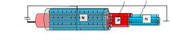
Şekil 1: Buluşun dışında üretilen maddelerden yapılan ve kullanılan transistörlerin ve buluş kapsamında kullanılan N-tipi ve P-Tipi lifler ve iplikler ile iletken metal ipliklerden yapılan NPN tipi transistörün  işleyiş mantığını  açıklayan model.

Şekil 2: NPN tipi katkılanan yarıiletken liflerden oluşan iplik ve yüklenen elektriğin hareket yönünü gösteren şema.

Şekil 3:  N ve P tipi ipliklerin NPN düzeninde bükülmesi.

Şekil 4:  üzeri yalıtkan malzemeyle kaplı NPN tipi ekose Kumaş Panel transistör.

Şekil 5:  üzeri yalıtkan malzemeyle kaplı NPN tipi Kumaş panel transistör.

Şekil 6: Buluşun dışında üretilen maddelerden yapılan ve kullanılan transistörlerin ve buluş kapsamında kullanılan N-tipi ve P-Tipi lifler ve iplikler ile iletken metal ipliklerden yapılan PNP tipi transistörün  işleyiş mantığını  açıklayan model.

Şekil 7:  PNP tipi katkılanan yarıiletken liflerden oluşan iplik ve yüklenen elektriğin hareket yönünü gösteren şema.

Şekil 8:  P ve N tipi ipliklerin PNP düzeninde bükülmesi.

Şekil 9 : üzeri yalıtkan malzemeyle kaplı PNP tipi ekose Kumaş Panel transistör.

Şekil 10:üzeri yalıtkan malzemeyle kaplı PNP tipi Kumaş panel transistör.


Şekillerin referansların açıklaması

1        : N-Tipi yarıiletken lif. (kollektör)

2        : P-Tipi yarıiletken lif.(Beyz)

3        : N-Tipi Yarıiletken lif.(Emiter)

4        : N ve P-Tipi liflerin biraraya getirilmesi veya bükülmesi ile oluşan iplik.

5        : Lif veya ipliklerin dış yüzeyinin yalıtkan madde ile kaplanması

6        : N-Tipi yar iletken lif. (kollektör)

7        : P-Tipi yarı iletken lif.(Beyz)

8        : N-Tipi yarıiletken lif.  (Emiter)

9        :P-Tipi yarıiletken ipliklerin dokuma kumaş üzerinde atkı çözgü yönündeki dizilişi (Beyz)

10    :N-Tipi yarıiletken ipliklerin dokuma kumaş üzerinde atkı çözgü yönündeki dizilişi

11    :İletken metal ipliklerin dokuma kumaş üzerinde atkı çözgü yönündeki   dizilişi veya nakışla işlenmiş görünüşü

12    :Yalıtkan ipliklerin dokuma kumaş üzerinde atkı çözgü yönündeki dizilişi

13    : Elektrik akımı yükleme anahtarı

14    : PNP tipi transistör de  P-Tipi alt iplik grubu dizilişi Kollektör)

15    : PNP tipi transistor de  N-Tipi  orta iplik grubu(Beyz) dizilişi

16    : PNP tipi transistor de  P-Tipi üst iplik grubu dizilişi (Emiter)

17    : PNP tipi  transistör grubunun yalıtkan madde ile kaplanması.

18    : PNP tipi transistör de büküme giren P-Tipi alt iplik grubu (Kollektör)

19    : PNP tipi transistor de büküme giren N-Tipi  orta iplik grubu(Beyz)

20    : PNP tipi transistor de büküme giren P-Tipi üst iplik grubu (Emiter)

21    : PNP tipi bükümlü transistör grubunun yalıtkan madde ile kaplanması

22    : Elektrik akımının girdiği metal iplik veya telden dağıtım kanalı

23    : Kumaş panelini çevreleyen yalıtkan iplikle dokunan veya örülen  alan

24    : P-Tipi yarıiletken ipliklerin dokuma kumaş üzerinde atkı çözgü yönündeki dizilişi

25    : N-Tipi yarıiletken ipliklerin dokuma kumaş üzerinde atkı çözgü yönündeki dizilişi

26    : PNP tipi transistör kumaş panelinin elektrik akımı iletimini sağlayan metal iplik  

              dokuma veya nakış işlemesi

27    : PNP tipi  transistör  kumaş panelinin  yalıtkan madde ile kaplanması.

      28  : metal iplik veya tellerin dokuma ve/veya nakış yoluyla işlenmesi.

Buluşun Açıklaması    :

A- Buluş, monokristalize veya kristalize saf silisyum veya kristalize saf silisyum veya kristalize silikon hammaddesi ve/veya monokristalize veya kristalize Germanyum ve/veya monokristalize veya kristalize cam hammaddesinin periyodik cetvelin 3.grup ve 5.grup elementleri ve/veya bileşik kimyasal katkı elementlerinin harmonizesinden veya katkılanmasından  elde edilen normal veya kristalize silikon elyafı ve/veya normal veya kristalize cam elyafı veya cam yününden devamlı veya kesikli normal veya kristalize 3.grup(P-Tipi)  silikon ve devamlı veya kesikli normal veya kristalize 5.grup (N-Tipi)silikon  nano ölçekten başlayıp en yüksek denyeye kadar silikon ve/veya cam elyaflarından üretilen (P-Tipi)ve (N-Tipi) ipliklerin ile baryum alüminyum borosilikat olarak adlandırılan çok ince bir endüstriyel cam  ve/veya Baryum ve alüminyum elementinin türevlerinden ve silisyum –bor karışımından veya Germanyum ve/veya bileşiklerinden veya diğer her türlü devamlı ve/veya kesikli liflerin çeşitli kimyasal işlemden geçerek Periyodik cetvelin 13.ve 15.grubundan başta 5 Atom no.lu Bor ve  15 atom no.lu fosfor olmak üzere elementlerle harmonizesi ve/veya  katkılanması veya emdirme yoluyla katkılanması ile üretilen ipliklerle elektrik akımını yükselterek akım ve gerilim kazancı sağlayan transistör üretimi ve/veya buluş kapsamında üretilen (P-Tipi) ve (N-Tipi) ipliklerle ve elektrik akımının iletilmesini sağlayan iletken metal iplik veya hertürlü iletken lif veya iplik veya iletken metallerle tekniğin bilinen dokuma tezgahlarında ve/veya örgü makinelerinde ve/veya brode ve raşel makinelerinde dokuma kumaş  haline getirilmesi ve/veya bu kumaşların nakış makinelerinde takviyeli işlenmesi  suretiyle oluşturulan hücre ve/veya bu hücrelerden meydana gelen dış yüzeyi yalıtkan kaplı NPN tipi ve/veya PNP tipi yarıiletken panellere yüklenen elektrik akımını yükselterek akım ve gerilim kazancı sağlanmasına matuf tekstil esaslı transistör cihazıdır.


B-Buluş, güneş enerjisi başta olmak üzere her türlü yenilenebilir enerji kaynakları ile petrol ve türevlerinden  ve diğer tüm kimyasal yollarla doğal ve yapay yollarla elde edilen elektriğin N-Tipi ve P-Tipi  devamlı ve/veya kesikli liflerin ve/veya hem N-tipi ve hem de P-Tipi katkılı kristalleri içinde barındıran liflerden doğrudan ve/veya N ve P tipi liflerden ve/veya hem N ve hem de P tipi kristalleri içinde barındıran liflerden oluşan bükümlü yada bükümsüz iplikler ile dokunan ve/veya örülen paneller vasıtasıyla P-Tipi ve N-Tipi paneller arasında oluşan atomların birbirlerini tetiklemesi ve baskısı ile yer değiştirmesi ile oluşan hareketliliğinde bu panellere yüklenen elektrik akımının yükseltilerek akım ve gerilim kazancı sağlanmasına matuf dış yüzeyi yalıtkan kılıfla kaplı tekstil esaslı transistör  cihazıdır.


C-  N-Tipi ve P-Tipi lif yada ipliklerle üretilen NPN tipi transistörün işleyişi şu şekildedir. NPN tipi transistörlerin yapısı iki N tipi yarı iletken liflerden ve ipliklerden oluşan madde arasına ince bir katman halinde yerleştirilmiş P tipi yarı iletken lif ve ipliklerden teşekkül eden beyz maddesinden oluşmaktadır. İki N tipi lif ve iplikler  arasındaki beyz tabakası elektron geçişini kontrol etme görevi yapar. Tekstil esaslı bu yapıdaki Transistor   geçen akımı denetleyerek küçük akımları büyütebilir ya da küçük bir akım ile büyük bir alıcının çalışmasını sağlayabilir.
NPN tipi transistörlerde şekil:1’de  görüldüğü gibi Vbb kaynağının artı ucu beyz kutbunu pozitif yüklerken Vcc kaynağının eksi ucu da  emiter kutbundaki elektronları yukarı iter. Sıkışan elektronlar beyz tarafından çekilir.Emiterin iletim bandındaki elektronlar E-B gerilim setini aşarak beyz bölgesine girerler, ancak ,beyz bölgesi dar olduğundan emiter bölgesinden gelen elektronların yaklaşık %2-3 ‘ü beyz bölgesi tarafından çekilirken kalan %97-98’i kollektöre geçer. Vcc kaynağının artı ucu elektronları kollektör bölgesine doğru çeker ve elektron akışı sürekli hale gelir ve Vbb kaynağının verdiği beyz akımının devamı  sürdükçe emiterden kollektöre elektron akışı devam eder. NPN tipi transistörlerde elektronlar yukarı, oyuklar ise aşağı doğru gider ve bu nedenle beyze uygulanan artı sinyal kollektörden emitere doğru akım geçirir . Emiter akımının beyz ve kollektör akımlarının toplamına eşit olduğu bilinmektedir.


D- P-Tipi ve N-Tipi lif yada ipliklerle üretilen PNP tipi transistörlerin yapısı da aynı  NPN tipi transistörlerdeki gibidir. Aradaki fark , bu kez P tipi iki yarı iletken oluşan lifler veya ipliklerin arasına ince bir tabaka halinde N tipi yarı iletken oluşan lifler yada ipliklerin yerleştirilmiş olmasıdır. PNP tipi transistörlerde Vbb kaynağının eksi ucu beyz kutbunu negatif yüklerken Vcc kaynağının artı ucu da emiter bölgesindeki artı yüklü oyukları yukarı iter. Bu şekilde sıkışan artı yükler beyz tarafından çekilip buradan kollektör bölgesine geçerler. Vcc kaynağının eksi ucu kollektör bölgesindeki oyukları kendine çektiğinden,  oyuk hareketi süreklilik kazanır. Vbb akımının devamlılığı  sürdükçe emiterden kollektöre doğru bu hareket sürer.PNP tipi transistörlerde elektronlar aşağı, oyuklar ise yukarı doğru gider ve bu nedenle beyze uygulanan eksi sinyal emiterden kollektöre doğru akım geçirir. Emiter akımının beyz ve kollektör akımlarının toplamına eşit olduğu da bilinmektedir.


Buluşun Sanayiye Uygulanma Biçimi

Yukarıda bahsedilen amaçlara hizmet eden, çevreye ve doğaya saygılı olarak her türlü üretilen elektriği en güvenli ve en az maliyetle buluş olan katkılı liflere ve bu liflerden oluşan panellere yükleyip  elektrik akımının yükseltilerek akım ve gerilim kazancı sağlanmasını sağlayan tekstil esaslı transistör olan bu cihazın , kolay ve güvenle ve yer kaplamayacak şekilde elektronik cihazlara monte edilmesi mümkün olup bu ürünün elde edilebilir hammaddeleri doğada bol bulunan ve bilinen maddelerdir. Ürün sanayinin başta tekstil ve enerji sektöründe ve/veya sanayinin herhangi bir dalında üretilebilir ve her alanda kullanılabilinir olup, sanayiye uygulanabilir yapıdadır.


                                                           İSTEMLER


1)      Buluş, (P-Tipi) lif  üretim yöntemi olup özelliği ; Yarı iletken monokristalize veya kristalize tek veya çok kristalli silisyum veya silikon maddesi ve/veya monokristalize veya kristalize cam maddesi veya periyodik cetveldeki diğer tüm yarı iletken elementler ve/veya bileşikleri ile periyodik cetvelin 3. grubundan (bor,aliminyum,galyum,indiyum, talyum, ununtriyum,holmiyum,aynştaynyum) elementlerinin saf veya bileşiklerinin katkılanması ile nano ölçekten başlayıp en yüksek  kalınlığa kadar tekniğin bilinen tekstil lifi üreten makinalarında devamlı veya kesikli tipte (P-Tipi) liflerin üretilmesi işlemine tabi tutulmasıdır.


2)      İstem 1’deki yöntem olup özelliği ; (P-Tipi) liflerin 2 veya daha fazlasının bir araya

getirilmesi ile emsal iplik cinslerinin numaralandırıldığı en düşük numaradan ve/veya nano ölçekli numaralardan başlamak üzere en yüksek numaraya  kadar tekstil esaslı ipliği içermesidir.


3)       Buluş, (P-Tipi) lif  üretim yöntemi olup özelliği ; Monokristalize veya kristalize Germanyum elementi ile periyodik cetvelin 3.grubundan Galyum elementinin saf veya bileşiklerinin katkılanması ve/veya periyodik cetvelin 3.grubunun diğer elementlerinin saf veya bileşiklerinin bir veya birkaçı ile nano ölçekten başlayıp en yüksek  kalınlığa kadar tekniğin bilinen tekstil lifi üreten makinalarında devamlı veya kesikli tipte  (P-Tipi) liflerin üretilmesi işlemine tabi tutulmasıdır.


4)      İstem 3’deki yöntem olup özelliği ; (P-Tipi) liflerin 2 veya daha fazlasının bir araya

getirilmesi ile emsal iplik cinslerinin numaralandırıldığı en düşük numaradan ve/veya nano ölçekli numaralardan başlamak üzere en yüksek numaraya  kadar tekstil esaslı ipliği içermesidir

5)       Buluş,(N-Tipi) lif  üretim yöntemi olup özelliği ;Yarıiletken monokristalize veya kristalize tek veya çok kristalli silisyum veya silikon maddesi ve/veya monokristalize veya kristalize cam maddesi veya periyodik cetveldeki diğer tüm yarı iletken elementler ve/veya bileşikleri ile periyodik cetvelin 5. grubundan (Azot,fosfor,arsenik,antimon,bizmut, ununpentiyum) elementlerinin saf veya bileşiklerinin katkılanması ile veya  monokristalize veya kristalize Germanyum elementi ile periyodik cetvelin ….grubundan Lityum elementinin saf veya bileşiklerinin katkılanması ile nano ölçekten başlayıp en yüksek  kalınlığa kadar tekniğin bilinen tekstil lifi üreten makinalarında devamlı veya kesikli tipte  (N-Tipi) liflerin üretilmesi işlemine tabi tutulmasıdır. 


6)      İstem 5’deki yöntem olup özelliği ; (N-Tipi) liflerin 2 veya daha fazlasının bir araya getirilmesi ile emsal iplik cinslerinin numaralandırıldığı en düşük numaradan ve/veya nano ölçekli numaralardan başlamak üzere en yüksek numaraya  kadar tekstil esaslı ipliği içermesidir


7)      Buluş,(N-Tipi) lif  üretim yöntemi olup özelliği ; Monokristalize veya kristalize Germanyum elementi ile periyodik cetvelin 5.grubundan Arsenik elementinin saf veya bileşiklerinin katkılanması ve/veya periyodik cetvelin 5.grubunun diğer elementlerinin saf veya bileşiklerinin bir veya birkaçı ile nano ölçekten başlayıp en yüksek  kalınlığa kadar tekniğin bilinen tekstil lifi üreten makinalarında devamlı veya kesikli tipte  (N-Tipi) liflerin üretilmesi işlemine tabi tutulmasıdır.


8)      İstem 7’deki yöntem olup özelliği ; (N-Tipi) liflerin 2 veya daha fazlasının bir araya getirilmesi ile emsal iplik cinslerinin numaralandırıldığı en düşük numaradan ve/veya nano ölçekli numaralardan başlamak üzere en yüksek numaraya  kadar tekstil esaslı ipliği içermesidir.


9) İstem NPN tipi Tekstil ipliği esaslı transistör üretim yöntemi olup özelliği; Şekil 1’deki modelde olduğu gibi, İstem 5 ve 7’deki  işlem adımları ile elde edilen (N-Tipi) 2 veya daha fazla liflerin en içte kalacak şekilde kendi aralarında bükümlü (5)ve/veya bükümsüz(1) işleme tabi tutularak bir araya getirilmesi ve bu liflerin üzerine istem1’deki  işlem adımları ile elde edilen (P-Tipi)  2 veya daha fazla liflerin, (N-Tipi) liflerin üzerine bükümlü (6)veya bükümsüz(2) sarılacak  şekilde işleme tabi tutulması ve orta tabakayı  teşkil eden (P-Tipi)  liflerin üzerine de gelecek şekilde (N-Tipi) 2 veya daha fazla liflerin bükümlü (7)ve/veya bükümsüz (3)olarak en üste sarılacak şekilde işleme tabi tutularak  şekil:2’de ve şekil:3’de olduğu gibi, yapılan bu işlemlerle  N-Tipi yarıiletken lif. (kollektör) (1) , (N-Tipi) Yarıiletken lif (Emiter) (3)liflerden oluşan düzenek arasına ince  bir katman halinde yerleştirilmiş P- Tipi yarıiletken liflerden (Beyz)(2) teşekkül eden beyz maddesinden ve düzeneğin dış yüzeyinin tamamının yalıtkan madde ile kaplanmasından (4),(8)NPN tipi iplik  transistör oluşmaktadır.NPN tipi transistor de İki N- tipi liflerden oluşan düzenek arasındaki P-tipi  liflerden oluşan beyz tabakası (2) elektron geçişini kontrol etme görevi yaparak buluşa ait, tekstil esaslı iplik şeklinde üretilen bu transistörün yaptığı iş , akımı denetleyerek küçük akımları büyütebilmesi ya da küçük bir akım ile büyük bir alıcının çalışmasını sağlamasıdır.

10) İstem 9’daki yöntem olup özelliği ; İstem 9’da nano ölçekten başlamak üzere en  yüksek kalınlığa kadar üretilen NPN tipi transistör esaslı ipliklerin (Beyz) teşkil eden P-Tipi liflerine (+) . (Emiter) teşkil eden ipliğin en üstünde sarılı N- Tipi liflerine (-)kutuplar bağlanarak elektrik yükü verilmesi ile ipliğin en altında sarılı olan ve ipliğin (Kollektör) kısmını teşkil eden N-Tipi liflerine Beyz’in elektron yapısının sıkıştırılması ile  geçen  elektriğin küçük (+) akımlarını büyütülmesi ile artan (+) akım sağlanması  ve  ipliğe kutuplar bağlanarak verilen elektrik yükünün hiçbir life uğramadan doğrudan akım gönderilen(-) akımlarının cihaz tarafından büyütülen (+)akımlarının bir uçta birleşmesi ve yüklerin dışa aktarılması  neticesinde büyük bir alıcının çalışmasının sağlanmasıdır. (şekil:1-şekil:2)    

11)İstem PNP tipi tekstil ipliği esaslı transistör üretim  yöntemi olup özelliği; Şekil 6’daki modelde olduğu gibi, İstem 1 ve 3’deki işlem adımları ile elde edilen (P-Tipi) 2 veya daha fazla liflerin en içte kalacak şekilde kendi aralarında bükümlü(19) ve/veya  bükümsüz(15) işleme tabi tutularak bir araya getirilmesi ve bu liflerin üzerine istem5’deki  işlem adımları ile elde edilen (N-Tipi)2 veya daha  fazla liflerin (P-Tipi) liflerin üzerine bükümlü (20)veya bükümsüz(16) sarılacak şekilde işleme tabi tutulması ve orta tabakayı teşkil eden (N-Tipi) liflerin üzerine de gelecek şekilde (P-Tipi) 2 veya daha fazla liflerin bükümlü (21)ve/veya bükümsüz(17) olarak en üste sarılacak şekilde işleme tabi tutularak  şekil:6’da ve şekil:7’de olduğu gibi,yapılan bu işlemlerle  P-Tipi yarıiletken lif. (kollektör)(15) , (P-Tipi) Yarıiletken lif (Emiter) (17) liflerden oluşan düzenek arasına ince bir  katman halinde yerleştirilmiş N- Tipi yarıiletken liflerden (Beyz)(16) teşekkül eden beyz  maddesinden ve düzeneğin dış yüzeyinin tamamının yalıtkan madde ile kaplanmasından (18),(22)  PNP tipi iplik  transistör oluşmaktadır. PNP tipi transistor de İki P- tipi liflerden oluşan düzenek arasındaki N-tipi  liflerden oluşan beyz tabakası (2) elektron geçişini kontrol etme görevi yaparak buluşa ait, tekstil esaslı iplik şeklinde üretilen bu transistörün yaptığı iş, akımı denetleyerek küçük akımları büyütebilmesi  ya da küçük bir akım ile büyük bir  alıcının çalışmasını sağlamasıdır.

 12) İstem 11’deki yöntem olup özelliği ; İstem 11’de nano ölçekten başlamak üzere en yüksek kalınlığa kadar üretilen PNP tipi transistör esaslı ipliklerin (Beyz) teşkil eden N-Tipi liflerine (-) . (Emiter) teşkil eden ipliğin en üstünde sarılı P- Tipi liflerine (+)kutuplar bağlanarak elektrik yükü verilmesi ile ipliğin en altında sarılı olan ve ipliğin (Kollektör) kısmını teşkil eden P-Tipi lifleri(Beyz)’e verilen (-) yükün sıkıştırılması  ile  elektriğin küçük (-) akımlarının büyütülmesi ile artan  (-) akım sağlanması  ve ipliğe kutuplar bağlanarak verilen elektrik yükünün hiçbir life uğramadan doğrudan akım gönderilen(+) akımlarının cihaz tarafından büyütülen (-)akımlarının bir uçta birleşmesi ve yüklerin dışa aktarılması neticesinde büyük bir alıcının çalışmasının sağlanmasıdır. (şekil:6 -şekil:7)

 13)Yukarıdaki istemlerde bahsedilen yöntem olup özelliği ;İstem 1,2,3,4,5,6,7,8‘dekiNPN tipi transistörlerin yapısıni oluşturmak üzere şekil:4 ve şekil:5’deki dokuma kumaşlarda olduğu gibi, N-Tipi yarıiletken iplikler(kollektör) (1), N-Tipi Yarıiletken iplikler(Emiter) (3) ipliklerden oluşan atkı ve çözgü dizilişi arasına ince bir katman halinde atkı ve çözgüipliklerinden oluşturulan P-Tipi yarıiletken(Beyz)(2) ipliklerinden teşekkül eden ipliklerden oluşmaktadır.N-Tipi yarı iletken ipliklerin dokuma kumaş üzerinde atkı çözgü yönündeki dizilişi (10) arasındaki P-Tipi yarıiletken ipliklerin dokuma kumaş üzerinde atkı çözgü yönündeki(Beyz)tabakası(9)oluşturulacak şekilde dokuma tezgahları veya örgü makinelerinde  dokunan ve örülen ipliklerle elde edilen kenarları yalıtkan iplikle örülen (12) ve yalıtkan iplikler üzerinden iletken metal iplik veya tellerin dokuma ve/veya nakış yoluyla işlenerek (11) N-Tipi yarıiletken ipliklerin dokuma kumaş üzerinde atkı çözgü yönündeki dizilişlerine (10), N-Tipi yarıiletken ipliklerin dokuma kumaş üzerinde atkı  çözgü yönündeki dizilişi (12) elektron geçişini sağlayarak ve panellerin üzeri yalıtkan madde ile kaplanarak (27) ve kontrol etme görevi yaparak, buluşa ait, tekstil’den mamul dokuma veya örgü  esaslı bu transistorün yaptığı işlem geçen akımı denetleyerek küçük akımları büyütebilmesi  ya da küçük bir akım ile büyük bir alıcının çalışmasını sağlamasıdır.


14)Yukarıdaki istemlerde bahsedilen yöntem olup özelliği; İstem 1,2,3,4,5,6,7,8‘dekiPNPtipi transistörlerin yapısıni oluşturmak üzere şekil:9 ve şekil:10’daki dokuma kumaşlarda  olduğu gibi, P-Tipi yarıiletken iplikler(kollektör) (15), P-Tipi Yarıiletken iplikler(Emiter) (17) ipliklerden oluşan atkı ve çözgü dizilişi arasına ince bir katman halinde atkı ve çözgü ipliklerinden oluşturulan N-Tipi yarıiletken(Beyz)(16) ipliklerinden teşekkül eden ipliklerden oluşmaktadır. P-Tipi yarı iletken ipliklerin dokuma kumaş üzerinde atkı çözgü yönündeki dizilişi (26) arasındaki N-Tipi yarıiletken ipliklerin dokuma kumaş üzerinde atkı çözgü yönündeki(Beyz)tabakası (25)oluşturulacak şekilde dokuma tezgahları veya örgü makinelerinde  dokunan ve örülen ipliklerle elde edilen kenarları yalıtkan iplikle örülen (24) ve yalıtkan iplikler üzerinden iletken metal iplik veya tellerin dokuma ve/veya nakış yoluyla işlenerek (28) N-Tipi yarıiletken ipliklerin dokuma kumaş üzerinde atkı çözgü yönündeki dizilişlerine (25), P-Tipi yarıiletken ipliklerin dokuma kumaş üzerinde atkı çözgü yönündeki dizilişi(26) elektron geçişini sağlayarak ve panellerin üzeri yalıtkan madde ile kaplanarak (27) ve kontrol etme görevi yaparak, buluşa ait, tekstil’den mamul dokuma veya örgü  esaslı bu transistorün yaptığı iş   geçen akımı denetleyerek küçük akımları büyütebilmesi  ya da küçük bir akım ile büyük bir alıcının çalışmasını sağlamasıdır.


İşbu sayfa ve eklentisi olan dosyalarda yayınlanan projeler Tubitak patent teşvik kapsamında ve 
patent koruması kapsamında olup,lisanslıdır. Bu projelerin izinsiz kullanılması, yayınlanması , dağıtılması ve alıntı yapılması yasaktır.Bu kurallara uymayanlar en ağır şekilde tazminat ve cezai yaptırımlarla cezalandırılır.      

Yorumlar - Yorum Yaz